Debugging Analysis of Kernel panics and Kernel oopses using System Map:

Linux Kernel Debugging Introduction:

There are various ways to debug an kernel like debugging by printing ,Using kernel symbols,Using a kernel debugger but this page describes some tricks and techniques to help Interpreting an Oops message and Kernel panic but before going forward we should understand what is kernel OOPS and panic.

A kernel panic is an action taken by an operating system upon detecting an internal fatal error from which it cannot safely recover and force the system to do a controlled system hang / reboot due to a detected run-time system malfunction (not necessarily an OOPS). The operation of the panic kernel feature may be controllable via run-time sysconfig settings such as hung task handling. This is a kernel panic.

OOPS are due to the Kernel exception handler getting executed including macros such as BUG() which is defined as an invalid instruction. Each exception has a unique number. Some “oops”es are bad enough that the kernel decides to execute the panic feature to stop running immediately. This is a kernel crash optionally followed by invoking a panic.

When a Kernel OOPS is encountered in a running kernel an OOPS message like ([ 67.994624] Internal error: Oops: 5 [#1] XXXXXXXXXXX) is displayed on the screen. The OOPS message contains the following: the values of the CPU registers, the address of the function that invoked the failure i.e PC, the stack, and the name of the current process executing. By using this OOPS statement, you can begin to debug the specific problem in the kernel. However, sometimes this OOPS message is insufficient.

How to interpret oopses with System.map

In Linux, the System.map file is a symbol table used by the kernel.

The System.map is required when the address of a symbol name, or the symbol name of an address, is needed. It is especially useful for debugging kernel panics and kernel oopses. The kernel does the address-to-name translation itself when CONFIG_KALLSYMS is enabled so that tools like ksymoops are not required.

More detailed information can be found here System.map.

Note: Addresses inside System.map may change from one build to the next or in another word new System.map is generated for each build of the kernel however it is must to have System.map of the same Linux kernel on which Kernel panics/oopses has been reported to debug the problem.

Note in the kernel backtraces in the logs, the kernel finds the nearest symbol to the address being analysed. Not all function symbols are available because of inlining, static, and optimisation so sometimes the reported function name is not the location of the failure.

How to Debug Kernel panics and oopses:


67.994406] Unable to handle kernel paging request at virtual address 02120bc4
[   67.994495] pgd = 94240000
[   67.994553] [02120bc4] *pgd=00000000
[   67.994624] Internal error: Oops: 5 [#1] PREEMPT SMP ARM
[   67.994926] CPU: 0    Not tainted  (3.8.13.23-XXXXXXXX #1)
[   67.994996] PC is at add_range+0x14/0x6c
[   67.995056] LR is at XXXXXXX+0x38/0x44
[   67.995117] pc : [<80049F3C>]    lr : [<8004a1ec>]    psr: 20000013
[   67.995117] sp : 9423fd90  ip : 9423fda8  fp : 9423fda4
[   67.995176] r10: 00000000  r9 : 9423ff60  r8 : 8000da84
[   67.995233] r7 : 000041fd  r6 : 00000081  r5 : aa068088  r4 : aa068088
[   67.995290] r3 : ac8ceb80  r2 : 021ab618  r1 : 00000000  r0 : 02120bc0
[   67.995348] Flags: nzCv  IRQs on  FIQs on  Mode SVC_32  ISA ARM  Segment user
[   67.995406] Control: 10c5387d  Table: 2424004a  DAC: 00000015
[   67.995462] Process cat (pid: 1352, stack limit = 0x9423e238)
[   67.995518] Stack: (0x9423fd90 to 0x94240000)
[   67.995577] fd80:                                     aa068088 aa068088 9423fdb4 9423fda8

Here is the kernel backtrace where Kernel is crashing   at “add_range” function. (Actually nearest function symbol to the crash). Let’s analyze step by step.

1. Crash occurs at below location as per Back Trace.

PC is at add_range +0x14/0x6c

 2. Grep/find add_range() in System.map file and note down symbol name address i.e. 80049f28

#Linux-Kernel # grep add_range System.map 
80049f28 T add_range

3.Replace add_range symbol name address in “add_range+0x14” = 80049f28 + 0x14 = 80049F3C

4.“80049F3C” should be same as PC Address in the Back trace .Wow it is same so it means that Kernel version I am using and on which issue is reported is same (also depends on same .config settings). Let’s move to next step.

5.run objdump on vmlinux to get the disassembly and detail on objdump program and vmlinux can be fetched from below hyperlinks.

objdump: is a program for displaying various information about object files. For instance, it can be used as a disassembler to view executable in assembly form.

vmlinux: is a statically linked executable file that contains the Linux kernel in one of the object file formats supported by Linux, The vmlinux file might be required for kernel debugging, symbol table generation or other operations,

#objdump -D -S --show-raw-insn --prefix-addresses --line-numbers vmlinux > objdump

6.Find “add_range” in vmlinux.objdump and look for PC address calculated above i.e.   80049F3C

80049F3C <add_Range+0x14> e5903004  ldr     r3, [r0, #4]

7.The crash point can be identified below.

ldr     r3, [r0, #4] = r0+4 = 02120bc0+4 = 02120bc4 /*replace r0 with r0 register value from the Back Traces*

8.Wow ! This  is same as fault address

Unable to handle kernel paging request at virtual address 02120bc4

Conclusion: Here r0 is pointing to invalid address and from disassembly found out where r0 is pointing and found out why r0 is pointing to invalid address.

Using GDB to find the location where your kernel panicked or oopsed.

A quick and easy way to find the line of code where your kernel panicked or oopsed is to use GDB list command. You can do this as follows.

Let’s assume your panic/oops message says something like:


[  174.507084] Stack:
[  174.507163] 
ce0bd8ac 00000008 00000000 ce4a7e90 c039ce30 ce0bd8ac c0718b04 c07185a0
[  174.507380] 
ce4a7ea0 c0398f22 ce0bd8ac c0718b04 ce4a7eb0 c037deee ce0bd8e0 ce0bd8ac
[  174.507597] 
ce4a7ec0 c037dfe0 c07185a0 ce0bd8ac ce4a7ed4 c037d353 ce0bd8ac ce0bd8ac
[  174.507888] Call Trace:
[  174.508125] 
[<c039ce30>] ? sd_remove+0x20/0x70
[  174.508235] 
[<c0398f22>] ? scsi_bus_remove+0x32/0x40
[  174.508326] 
[<c037deee>] ? __device_release_driver+0x3e/0x70
[  174.508421] 
[<c037dfe0>] ? device_release_driver+0x20/0x40
[  174.508514] 
[<c037d353>] ? bus_remove_device+0x73/0x90
[  174.508606] 
[<c037bccf>] ? device_del+0xef/0x150
[  174.508693] 
[<c0399207>] ? __scsi_remove_device+0x47/0x80
[  174.508786] 
[<c0399262>] ? scsi_remove_device+0x22/0x40
[  174.508877] 
[<c0399324>] ? __scsi_remove_target+0x94/0xd0
[  174.508969] 
[<c03993c0>] ? __remove_child+0x0/0x20
[  174.509060] 
[<c03993d7>] ? __remove_child+0x17/0x20
[  174.509148] 
[<c037b868>] ? device_for_each_child+0x38/0x60
[  174.509241] 
[<c039938f>] ? scsi_remove_target+0x2f/0x60
[  174.509393] 
[<d0c38907>] ? __iscsi_unbind_session+0x77/0xa0
[scsi_transport_iscsi]
[  174.509699] 
[<c015272e>] ? run_workqueue+0x6e/0x140
[  174.509801] 
[<d0c38890>] ? __iscsi_unbind_session+0x0/0xa0
[scsi_transport_iscsi]
[  174.509977] 
[<c0152888>] ? worker_thread+0x88/0xe0
[  174.510047] 
[<c01566a0>] ? autoremove_wake_function+0x0/0x40

Lets say you want to know what line of code represents sd_remove+0x20/0x70. cd to your directory of your kernel tree and run gdb on the “.o” file which has the function sd_remove() in this case in sd.o, and use the gdb “list” command, (gdb) list *(function+0xoffset), in this case function is sd_remove() and offset is 0x20, and gdb should tell you the line number where you hit the panic or oops. This worked reliably for most cases.

#gdb sd.o
gdb)list *(sd_remove+0x20)
0x1650 is in sd_remove
(Kernel/linux-xxx/drivers/scsi/sd.c:2125).
2120    static int sd_remove(struct device *dev)
2121    {
2122            struct scsi_disk *sdkp;
2123    
2124            async_synchronize_full();
2125            sdkp = dev_get_drvdata(dev);
2126           
blk_queue_prep_rq(sdkp->device->request_queue, scsi_prep_fn);
2127            device_del(&sdkp->dev);
2128            del_gendisk(sdkp->disk);
2129            sd_shutdown(dev);
(gdb)

so dev_get_drvdata()is the function where crash has been happened and Lets analyze why dev_get_drvdata(dev)is crashing.


Disassembling the kernel

Cross tools are needed.

The objdump utility

The main utility used to do it is the objdump one.

arm-none-linux-gnueabi-objdump –dr vmlinux  /*If We have object code handy then, we can disassemble the individual object file also like objdump -S panic.o"

gdb on vmlinux

One can disassemble a built kernel using gdb on the vmlinux image. This is useful when one gets a kernel Oops message and a stack dump – one can then disassemble the object code and see where the Oops is occurring. For example:   

#arm-none-linux-gnueabi-gdb –silent vmlinux
#disassemble printk
Dump of assembler code for function printk:
0xffffffff8023dce0 <printk+0>:  sub    $0xd8,%rsp
0xffffffff8023dce7 <printk+7>:  lea    0xe0(%rsp),%rax
0xffffffff8023dcef <printk+15>: mov    %rsi,0x28(%rsp)
0xffffffff8023dcf4 <printk+20>: mov    %rsp,%rsi
0xffffffff8023dcf7 <printk+23>: mov    %rdx,0x30(%rsp)
0xffffffff8023dcfc <printk+28>: mov    %rcx,0x38(%rsp)
0xffffffff8023dd01 <printk+33>: mov    %rax,0x8(%rsp)
0xffffffff8023dd06 <printk+38>: lea    0x20(%rsp),%rax
0xffffffff8023dd0b <printk+43>: mov    %r8,0x40(%rsp)
0xffffffff8023dd10 <printk+48>: mov    %r9,0x48(%rsp)
0xffffffff8023dd15 <printk+53>: movl   $0x8,(%rsp)
0xffffffff8023dd1c <printk+60>: movl   $0x30,0x4(%rsp)
0xffffffff8023dd24 <printk+68>: mov    %rax,0x10(%rsp)
0xffffffff8023dd29 <printk+73>: callq  0xffffffff8023d980 <vprintk>
0xffffffff8023dd2e <printk+78>: add    $0xd8,%rsp
0xffffffff8023dd35 <printk+85>: retq   
End of assembler dump.


How to Interpret Assembly Language(EABI C function call mapping to ARM registers)

First of all we should disassemble the kernel function with either OBJDUMP utility or using gdb on vmlinux kernel image by referring above mention section in Document. For example here is the dis-assembly of add_range() kernel function where I will demonstrate how this all works.This will be different depending on how the compiler optimizes,but it should give an idea.

#gdb disassemble add_range
Dump of assembler code for function add_range:
   0x8004c4d8 <+0>:    mov    r12, sp
   0x8004c4dc <+4>:    push    {r4, r5, r6, r7, r11, r12, lr, pc}
   0x8004c4e0 <+8>:    sub    r11, r12, #4
   0x8004c4e4 <+12>:    ldrd    r6, [r11, #4]
   0x8004c4e8 <+16>:    ldrd    r4, [r11, #12]
   0x8004c4ec <+20>:    cmp    r7, r5
   0x8004c4f0 <+24>:    cmpeq    r6, r4
   0x8004c4f4 <+28>:    bcs    0x8004c510 <add_range+56>
   0x8004c4f8 <+32>:    cmp    r2, r1
   0x8004c4fc <+36>:    lsllt    r3, r2, #4
   0x8004c500 <+40>:    addlt    r2, r2, #1
   0x8004c504 <+44>:    addlt    r1, r0, r3
   0x8004c508 <+48>:    strdlt    r6, [r0, r3]
   0x8004c50c <+52>:    strdlt    r4, [r1, #8]
   0x8004c510 <+56>:    mov    r0, r2
   0x8004c514 <+60>:    ldm    sp, {r4, r5, r6, r7, r11, sp, pc}
End of assembler dump.

Corresponding Kernel C function.

int add_range(struct range *range, int az, int nr_range, u64 start, u64 end)
{
        if (start >= end)
                return nr_range;
        /* Out of slots: */
        if (nr_range >= az)
                return nr_range;
        range[nr_range].start = start;
        range[nr_range].end = end;
        nr_range++;
        return nr_range;
}

Lets analyse the first 3 lines which is more or less same/common across all functions and here r12=IP(Intra-Procedure-call scratch register),r11=FP(Frame pointer).The FP keeps track of the variables from function to function.It is a frame on the stack of the function.please explore basic frame layout for more detail.so in simple words SP is where the stack is and FP is where the stack was like PC and LR register.

 0x8004c4d8 <+0>:    mov    r12, sp   /*get a copy of sp*/
 0x8004c4dc <+4>:    push    {r4, r5, r6, r7, r11, r12, lr, pc} /*Save the frame,link register,program counter and other Register on to the stack */
 0x8004c4e0 <+8>:    sub    r11, r12, #4 /*Set the new frame pointer.*/

The next 2 instruction passing 4 bytes and 12 bytes from the Frame pointer into the r6 and r4 registers for an function call and in other words values stores at r11+#4 would be stored in r6 and values stores at r11+#12 would be stored in r4.

Note:LDRD is used to store Double Word instruction however content also will be loaded into r7 and r5 register.This function call is dealing with 64 bit data so 64 bit data is manipulated in stack only.

  0x8004c4e4 <+12>:    ldrd    r6, [r11, #4]
   0x8004c4e8 <+16>:    ldrd    r4, [r11, #12]

Note:The first four registers r0-r3 are used to pass argument values into a subroutine and to return a result value from a function.so R0=range,R1=az,R2=nr_range,R3=start,R4=end.

The next instructions  can easily mapped with c code

Note:Underlying mapping somewhat different from the normal C to Assembly conversion mapping because here 64-bit value is being passed in Function call argument which is u64 start and u64 end and to deal with 64 bit data it has to be stored in register pair and can be retrived using ldrd instruction from stack using  frame pointer.

 0x8004c4ec <+20>:    cmp    r7, r5    /*first instruction compare r7 and r5 register i.e store 32 bit LSB for start & End whose value is stored in stack.       
 0x8004c4f0 <+24>:    cmpeq    r6, r4  /*This next instruction performs an comparison only if the result of above  { cmp    r7, r5 } instruction found true(i.e r7=r5). 
 0x8004c4f4 <+28>:    bcs    0x8004c510 <add_range+56>
 0x8004c4f8 <+32>:    cmp    r2, r1   /*This instruction compare values stored in resisters r2 and r1 which are passed argument values i.e nr_range and az. 

Corresponding C code is 

if (start >= end)
                return nr_range;
/* Out of slots: */
        if (nr_range >= az)
                return nr_range;

Lets move to next instructions .

0x8004c4fc <+36>:    lsllt    r3, r2, #4 
0x8004c500 <+40>:    addlt    r2, r2, #1
0x8004c504 <+44>:    addlt    r1, r0, r3
0x8004c508 <+48>:    strdlt    r6, [r0, r3]
0x8004c50c <+52>:    strdlt    r4, [r1, #8]

Corresponding C code is 

range[nr_range].start = start;
        range[nr_range].end = end;
        nr_range++;


0x8004c510 <+56>:    mov    r0, r2 /*move r2 content into r0 register which can be return back and As I said R0-R3 are also used to hold return value from function.
0x8004c514 <+60>:    ldm    sp, {r4, r5, r6, r7, r11, sp, pc} /*LDM is used to load multiple instructions and similar to  POP stack instruction.

Corresponding C code is
 
    return nr_range;

Here are the ARM Register definition for your reference and please keep in mind these register when you are mapping C function to ARM registers and more detailed information can be found here.

Note:In addition to above technique’s,don’t forget to visit Tour of ARM Assembly(http://www.coranac.com/tonc/text/asm.htm ) which will help you to understand following’s in deeper detail and after going through it, I Bet you,you should be able to produce some nice ARM assembly, or at least be able to read it well enough.

  • General assembly

  • The ARM instruction set

References:

  1. Procedure Call Standard for the ARM® Architecture
  2. ARM Procedure Call Standard
  3. Arm Instruction set manual


Safety model/concept for the i.MX8 SOC

i.MX8 Series of Application processor has following families.  Below detail is provided with respect to safety only.

  1. i.MX 8 Advanced Graphics, Performance and Virtualization
  2. i.MX 8X Safety certifiable and efficient performance
  3. i.MX 8M Advanced Audio, Voice and Video
  4. i.MX 8M Mini Embedded Consumer and Industrial Applications

i.MX 8X family is the first i.MX offering to feature Error Correcting Code (ECC) on the DDR memory interface, combined with reduced soft-error-rate (SER) and increased latch-up immunity, opening new opportunities for innovative industrial and automotive applications.

Automotive safety certification is also supported up to ASIL-B for cameras and displays by leveraging an advanced SafeAssure® display controller with failover safety planes and a real time domain that is independent of the Cortex-A CPUs and 3D graphics accelerators. This is said to enable automotive safety certification of up to ASIL-B for cameras and displays.

Industrial safety certification is supported up to SIL 3 by leveraging ECC on the L2 cache and DDR3L memory interfaces, enabled by several popular commercial RTOS solutions from QNX, Green Hills and others. This should be out of scope for us, I believe.

i.MX 8X Key Features:

  • Safeguard Mission Critical Displays and Control Functions
    • Increase system accuracy – ECC to support SIL 3
    • Ensure your display stays up and correct – SafeAssure® ASIL-B ready HW protects critical info with fail-over-capability
    • Advanced programmable security
    • Improved system reliability with FD-SOI
    • Offload time-critical tasks

The platform is compliant with ASIL-B, ensuring that screens “stay up” even in the event of a system crash. This family supports up to 16 hardware-based firewall domains engineered to isolate crashes, external attacks, and other system level issues. The SoC’s “SafeAssure Fail-Over” display controllers monitor the system’s graphics pipeline in order to automatically transition to a fully isolated display path if necessary.

For more detail, we would need i.MX 8/8X Applications Processor Safety Manual. It is not public document so we need to contact NXP Distributor.

Additionally, Freescale has Functional Safety Solution program(SAFE ASSURE) helping design-in SafeAssure products and achieving system-level functional safety compliance. https://www.nxp.com/applications/solutions/automotive/functional-safety-and-security/safeassure-functional-safety-program:SAFETYPRGRM

ARM Trusted firmware

Introduction

This page would described ARM Trusted firmware and How this is different from TEE.

ARM Trusted Firmware provides a reference implementation of secure world software for Armv7-A and Armv8-A, including a Secure Monitor executing at Exception Level 3 (EL3). More detail can be found here https://github.com/ARM-software/arm-trusted-firmware

ATF and Trusted Execution Environment (TEE) both provides the secure world software and environment to ensure code/data integrity and confidentiality for safely deploy applications that require handling confidential information. But Question is how they are different from each other ?

ATF Vs TEE

On an ARMv7 based processor,with TEE using TrustZone technology, TrustZone enables a single physical processor core to execute normal world (Rich OS like Linux/Android) and the secure world (Security OS like OP-TEE).  This communication/switching between secure and non-secure world is built-in to OP-TEE for ARMv7 platforms.

On an ARMv8 platform, ARM Trusted firmware provides the monitor code to manage the switch between secure and non-secure world.

An open source home automation solution

A wide variety of home automation solutions are being developed – but most of them require professionals and skilled staff to install and/or operate them. Furthermore, most of these solutions lack the potential for seamless integration into an already functioning home environment. To bridge the gap between consumer and expert, and to allow integration into any existing home environment without physical alteration to the building, a modular home automation solution with seamless integration potential is required.

The proposed system uses open source software and hardware, allowing for development to continue within the existing open source community. This type of system can be installed and configured without professional skills or physical alteration of the environment itself, due to its modular design and flexibility.

A smart home automation system, by definition, is the integration of electrical devices (including actuation of non-electrical devices such as blinds) and the monitoring and control of the home environment through an intelligent system or by a user over a communication medium, such as Bluetooth or Wi-Fi, and coordinated by a computer.

Within this connected environment, tasks can be made more intuitive and effective. The home network handles all communication and a user is given access to the system via a personal computer, smartphone, or tablet from either within the home or from a remote location over the Internet. The integration of information technologies into the home environment allows systems and appliances to function with convenience, energy efficiency, and safety benefits. The overall smart home architecture therefore consists of the devices and appliances within the home connected to the home network, the user, and the industry service providers.

Existing smart home automation systems are uniquely designed to suit specific consumers home environments and requirements. These systems are complex in design, not flexible enough to meet the custom requirements, and are often embedded into the physical structures of the home – they are also expensive, which prevents adoption by the average consumer and limits the potential for reconfiguration and expansion in order to satisfy the changing needs of the consumer. In addition, the exclusion of open source software also prevents the growth and expansion of smart home automation system.

To solve these problems, a seamlessly integratable, open-source-software-based, reconfigurable and expandable smart home automation system is proposed. To serve as a platform upon which research can continue, it should make maximum use of open source hardware and software. It should also allow for multiple configurations of sensors and actuators and be easy to modify, resulting in a modular design. This will allow the third party community and every customer to reconfigure the system such that it suits the requirements of each unique household.

More detail can be found On Embedded Computing Design

 http://www.embedded-computing.com/iot/a-home-automation-solution

UTTAR PRADESH AOA’s/RWA REGISTRATION/RENEWEL PROCEDURES

REGISTRATION PROCEDURES

Association of Apartment Owners (AOAs) & RWA are the organization run for the non-profit motive. A Resident welfare organization or say RWA is the committed to take care and development of a particular locality. The Resident Welfare Organization (RWA) is NOT a government body or government organ.

In India RWA & AOAs formation is covered under SOCIETIES REGISTRATION ACT, 1860. Steps involved to register a AOA’s & Resident Welfare Organization (RWA ) under society registration act differs between States to States as all the States have adopted the above mentioned act with some changes. In this post, I am going to discuss the procedure involved to register an Association of Apartment Owners (AOAs) or Resident Welfare Organization (RWA) under society registration act.

In Uttar Pradesh, Societies are registered with the Registrar of Firms, Societies and Chit. The detailed procedure is given below:

  • Cover Letter
  • Instructions for Cover Letter
  • Drafted Affidavit/NOC by Builder
  • First get at least 7 members for formation of a society.
  • Draft a Memorandum of Association and By-Laws of the society in duplicate with signatures of at least 3 members on all the papers.
  • The Memorandum and By-Laws are strictly to be as per the guidelines in Society Registration Act and should be only for charitable purpose.
  • Take the address proof of all the members of the society and one of the registered address of the society.
  • Draft a Board Resolution where all the members had desired to form a society together with a approval of name of the society.
  • Make a affidavit at Rs. 10 stamp paper saying that the Society name proposed is not used by any other society and the address of the society is correct.
  • File all the above documents with a fees of Rs. 2000 (fees is as per January, 2013 but may get revised afterwards)

RENEWAL PROCEDURES

Every Society registered under above act is valid for five years. After that, the body has to be renewed for another five years.

Note: It is always good to renew Society registration before your due date.

In Uttar Pradesh, Societies are registered with the Registrar of Firms, Societies and Chit. REGISTRATION RENEWEL should be straight forward but Many AOAs are faced with a peculiar problem — despite completing all formalities the members have failed to get their associations renewed, and some are pending renewal for over a year now.

Every time the AOAs approach the deputy registrar’s office in Meerut, they are handed out a new list of documents that are to be submitted to get the registration renewed.

doc

The detailed procedure for renewal is given below:

Here are the list received from the Registrar office and according to this list, following document shall be furnished along with the application for the renewal of the existing registration certificate of a society.

doc1
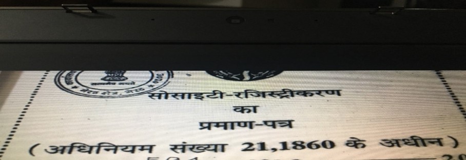
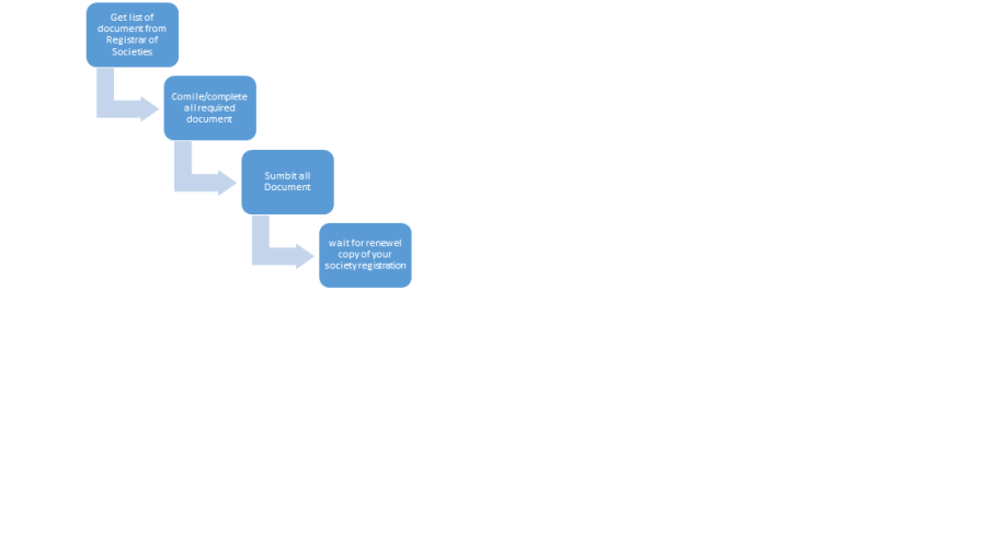
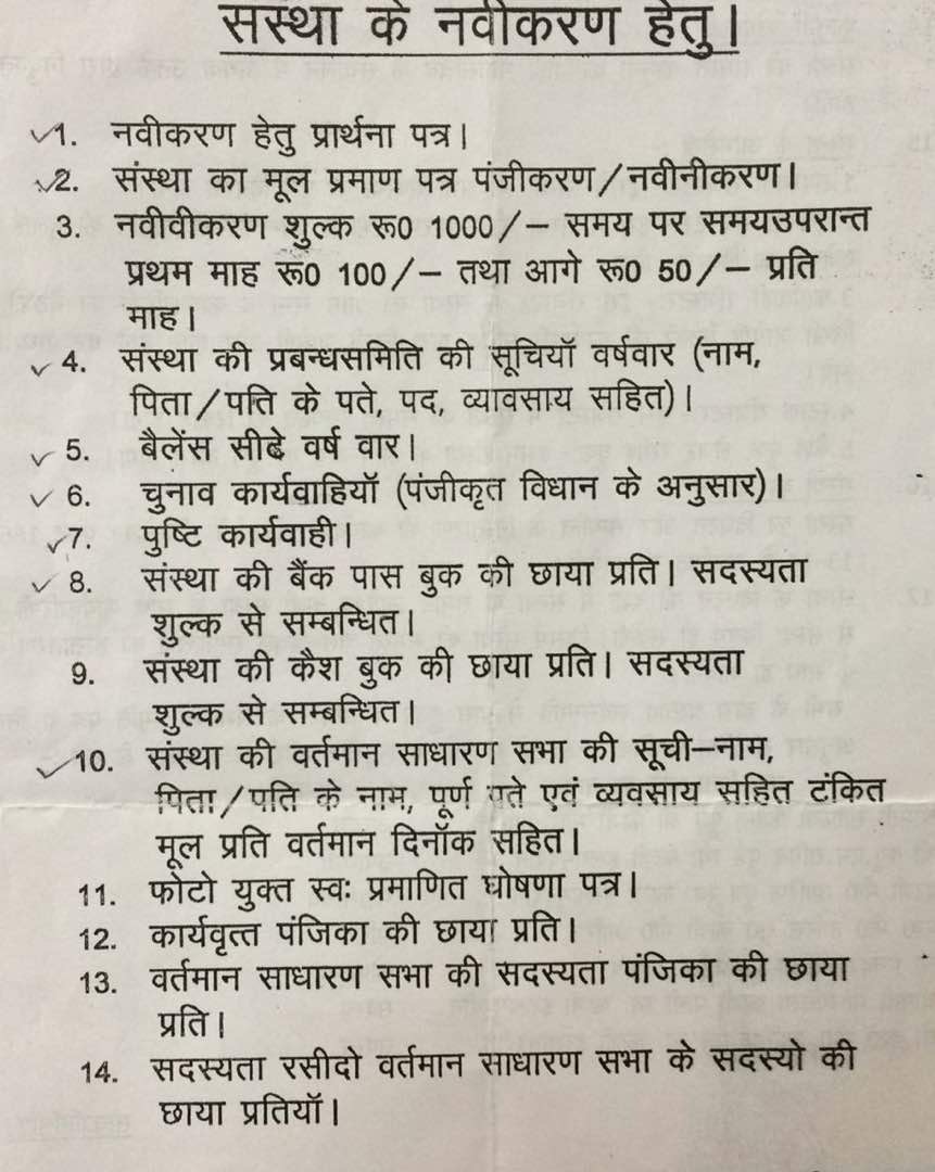
1.Application for Renewal on prescribed form if any. This request should be placed on RWA/AOA Letter Head and duly signed by Secretary. Every application of renewal of registration certificate shall be accompanied by:

  • Model Bye laws duly signed by RWA Executive body.
  • Relevant resolution of the General Body meeting for the purpose.

2.  Original Society Registration Certificate.

doc2

3. Renewal fees Rs. 1000/-(One Thousand) within the renewal due date. Please check above list for late fee after renew date expired.

4. The names, addresses, occupations and designations of the present members of the Governing Body of the AOA/RWA. Here is the format for your reference.

                             List of  present members of RWA/AOA Year()
Sr.no Name Father/Husband Address Post/Designation Occupation
 1.  XXX  XXX  XXX  XXX  XXX
 2.  XXX  XXX  XXX  XXX  XXX

5. Annual Balance sheet for every year.

6.Election Notification.

7. Election proceedings as per Registered By laws.

8. Photocopies of all pages of the Bank Pass-Book of the society

9.Cash book of the society, relating to the preceding three year or five year, pending the date of renewal application.

10.Current resident list in below format. We also need to mention RWA Membership fees which is mentioned 500 in our case. It may different in your case. Please change accordingly.

                                      Society Resident  List
Sr. Name Father/Husband Address Occupation Membership Type Membership Receipt  Fee Received
 1 XXX XXX XXX XXX XXX XXX XXX
 2 XXX XXX XXX XXX XXX XXX XXX

 11. AAdhar card of all the office bearer and executive member of RWA duly signed by individually.

12.MOM of the EB and GBM Meetings.

13. RWA Membership Receipt Book.

14. RWA Membership receipt of the Residents at joining of RWA.here is the reference

doc6

15. Self-declaration

doc3

After submission of all document you will get following receipt from Registrar of Societies.

doc4


doc5

Information Technology, FDI& Economic Growth in India: An Overview

Sanjeev Sharma

E-mail : sanjeev_sharma@mentor.com

MENTOR GRAPHICS https://www.mentor.com/

Abstract

Foreign Direct Investment is fund flow between the countries in the form of inflow or outflow by which one can able to gain some benefit from their investment whereas another can exploit the opportunity to enhance the productivity and find out better position through performance. The effectiveness and efficiency depends upon the investors perception, if investment with the purpose of long term then it is contributes positively towards economy on the other hand if it is for short term for the purpose of making profit then it may be less significant. The FDI may also affect due to the government trade barriers and policies for the foreign investments and leads to less or more effective towards contribution in economy also in GDP of the economy as well as information technology sector. This paper conducts an empirical analysis of India using time series data to see if there is empirical evidence that supports this assumption.


Objectives

The research paper covers the following objectives:

  • To study the impact of FDI on IT.
  • To study the pattern of flow of FDI.
  • To assess the determinants of FDI inflows.


Introduction

foreign direct investment (FDI) is an investment made by a company or entity based in one country, into a company or entity based in another country.

Foreign Direct Investment (FDI) in India is the major monetary source for economic development in India. Foreign companies invest directly in fast growing private Indian businesses to take benefits of cheaper wages and changing business environment of India.


Foreign investment was introduced in 1991 under Foreign Exchange Management Act (FEMA), driven by the finance minister Manmohan Singh. As Singh subsequently became the prime minister, this has been one of his top political problems, even in the current times. India disallowed overseas corporate bodies (OCB) to invest in India. India imposes cap on equity holding by foreign investors in various sectors, current FDI in aviation and insurance sectors is limited to a maximum of 49%.

The success of Indian software industry has captured the imagination of both Indian and the world. For a country, attracting an inflow of FDI strengthen the connection to world trade networks and finance its development path. Foreign investment plays a significant role in development of Indian economy. Foreign direct investment acts as a bridge to fulfill the gap between investment and saving. Many countries provide many incentives for attracting the foreign direct investment. A foreign direct investor may be classified in any sector of the economy and could be any one like an individual, a group of related individuals, a public company or a private company, a government body or any combination of these. IT can potentially be used in every sector of the economy. The true impact of IT on growth and productivity continues to be a matter of debate, even in the United States, which have been the leader and largest adopter of IT. There is no doubt that the IT sector has been a dynamic one in many developed countries, and in a developing country like India it has stood out in the guise of software exports, despite the country’s relatively low level of income and development.


Foreign Direct Investments in India

Foreign companies invest directly in fast growing private Indian businesses to take benefits of cheaper wages and changing business environment of India. Foreign companies invest in India to take advantage of relatively lower wages, special investment privileges such as tax exemptions, etc. For a country where foreign investments are being made, it also means achieving technical know-how and generating employment.

FDI in India for Foreign Investors

Hotel & Tourism
Non-Banking Financial Companies
Insurance Sector
Telecommunication
Trading
Drugs & Pharmaceuticals
Small Scale Industries (SSI’s)

India is the world’s largest sourcing destination for the information technology (IT) industry, accounting for approximately 67 per cent of the US$ 124-130 billion market. The industry employs about 10 million workforces. More importantly, the industry has led the economic transformation of the country and altered the perception of India in the global economy. India’s cost competitiveness in providing IT services, which is approximately 3-4 times cheaper than the US, continues to be the mainstay of its unique selling proposition (USP) in the global sourcing market. However, India is also gaining prominence in terms of intellectual capital with several global IT firms setting up their innovation centers in India.


fdi


The IT industry has also created significant demand in the Indian education sector, especially for engineering and computer science. The Indian IT and ITeS industry is divided into four major segments – IT services, business process management (BPM), software products and engineering services, and hardware.

The IT-BPM sector in India grew at a Compound Annual Growth rate (CAGR) of 15 per cent over 2010-15, which is 3-4 times higher than the global IT-BPM spend, and is estimated to expand at a CAGR of 9.5 per cent to US$ 300 billion by 2020.


fdi1


Indian IT’s core competencies and strengths have attracted significant investments from major countries. The computer software and hardware sector in India attracted cumulative Foreign Direct Investment (FDI) inflows worth US$ 18.17 billion between April 2000 and September 2015, according to data released by the Department of Industrial Policy and Promotion (DIPP).  It is being discussed to deregulate FDI restriction further, policymaker in India as well as external observers attach high expectations to FDI. In the critical face of Indian economy the government of India with the help of World Bank and IMF introduced the macro-economic stabilization and structural adjustment program. As a result of these reforms India open its door to FDI inflows and adopted a more liberal foreign policy in order to restore the confidence of foreign constituted (Foreign Investment Promotion Board) whose main function was to invite and facilitate foreign investment. The government relaxed FDI norms in several sectors including telecom, defense, PSU oil refineries, and power exchanges, among others.

Here are the few statistics that shows the growth of IT and BPM industry in FDI.

  • IT-BPM revenues are expected to reach USD 146 Billion in 2015.
  • Exports from the IT-BPM industry are expected to reach USD 98.5 Billion in 2015.
  • IT Services exports are USD 55 Billion.
  • The BPM industry exports are USD 20 Billion.
  • The hardware industry exports are USD 0.4 Billion.
  • The IT industry has more than 15,000 firms; of which 1000+ are large firms.
  • The IT-BPM industry is the largest private sector employer – delivering 3.5 Million jobs.
  • The sector accounts for 38% of India’s services exports.
  • The sector includes 640 offshore development centers (ODCs) across around 78 countries.
  • India is ranked as the 9th largest start-up hub in the world with over 3100 start-ups in the country.


Policy Initiatives

The information technology industry of India has been attracting considerable amount of foreign direct investment in the recent years. Investments are being made in the four principal sectors of the Indian information technology industry – online businesses, information technology services, information technology based services and software merchandise.

Newer investment opportunities are opening up every now and then in the Indian information technology scenario. The government of India has released a comprehensive FDI policy document effective from 2010. The government has allowed the Foreign Investment Promotion Board (FIPB), under the Ministry of Commerce and Industry, to clear FDI proposals of up to US$ 258.3 million. Earlier all project proposals that involved investment of above US$129.2 million were put up before the Cabinet Committee of Economic Affairs (CCEA) for approval.

Mauritius remains the top investing country for India during the period from August 1991 to March 2014. Investments from the country amounted to US $82,133 million during this period followed by Singapore and Japan. It shows that there has been a significant shift in the character of global capital flows to the India in recent years in that the predominance of private account capital transfer and especially portfolio investment increased considerably.

fdi2


State wise FDI inflows show that Maharashtra, Delhi, Karnataka, Gujarat and Tamil Nadu together accounted more 75% of inflows during 2000-2015 because of the infrastructural facilities and favorable business environment provided by these states. Despite troubles in the world economy, India continued to attract FDI inflows mainly because Government of India open-up with flexible investment regimes and policies prove to be the horde for the foreign investors in finding the investment opportunities in the country.

As per Indian government recent FDI polices, up to 100% Foreign Direct Investment (FDI) is permitted under the automatic route in data processing, software development and computer consultancy services, software supply services, business and management consultancy services, market research services, technical testing and analysis services.In a big jump, India has moved up 16 positions to rank 55th on a global index of the world’s most competitive economies, where Switzerland remains on top.

EFFECT OF FDI ON IT SECTOR

The Indian Information Technology (IT) sector is expected to grow 11 per cent per annum and triple its current annual revenue to reach US$ 350 billion by FY 2025, as per National Association of Software and Services Companies (NASSCOM).India, the fourth largest base for new businesses in the world and home to over 3,100 tech start-ups, is set to increase its base to 11,500 tech start-ups by 2020, as per a report by NASSCOM and Zinnov Management Consulting Pvt Ltd.


India’s internet economy is expected to touch Rs 10 trillion (US$ 151.6 billion) by 2018, accounting for 5 per cent of the country’s gross domestic product (GDP), according to a report by the Boston Consulting Group (BCG) and Internet and Mobile Association of India (IAMAI). India’s internet user base reached over 350 million by June 2015, the third largest in the world, while the number of social media users grew to 143 million by April 2015 and smart phones grew to 160 million.


Public cloud services revenue in India is expected to reach US$ 838 million in 2015, growing by 33 per cent year-on-year (y-o-y), as per a report by Gartner Inc. In yet another Gartner report, the public cloud market alone in the country was estimated to treble to US$ 1.9 billion by 2018 from US$ 638 million in 2014. Increased penetration of internet (including in rural areas) and rapid emergence of e-commerce are the main drivers for continued growth of data centre co-location and hosting market in India.

BENEFITS OF FDI IN IT SECTOR

  • Sector grew by 12% in FY2009 to reach US$ 71.76 billion in aggregate revenue
  • Opportunities in Knowledge Process Outsourcing – India climbing the global value chain
  • India able to add value to global KPO – valuation research, investment research, patent filing, insurance claims processing, online teaching, legal process outsourcing
  • India projected to be the highest growth market in the APAC region with 11.4% growth in domestic IT spending in 2009
  • Increased M&A driven by need for global service delivery capabilities
  • IT sector emerged as the preferred space for venture capital investments in India
  • India estimated to garner a share of $50 billion by 2020 for engineering services


fdi3

Conclusion

One of the major advantages of this method is that the Indian information technology professionals are more viable from the economic point of view Since they are at par with the international standards as far as skills are concerned it is pretty easy to extract good work out of them. This has however helped in the expansion of the job market in India as an increasing number of people are landing jobs with the international information technology companies and are living better lives.Foreign direct investment in India’s information technology industry has also been contributed to by the remarkable growth of the industry in the recent years.


References

Ministry of Finance, Report of the economic survey, Government of India, New Delhi.

http://www.makeinindia.com/sector/it-and-bpm

www.google.com

http://www.ibef.org/industry/services.aspx

www.wikipedia.org

http://www.ibef.org/industry


NOTE:This paper is published in “Foreign Direct Investment and Socio-Economic Transformation in India” book by Shree Publishers and Distributors

Project Management Guide

Introduction

What is Project Management?

Project management is the application of knowledge, skills, tools, and techniques to project activities to meet the project requirements. Project management is accomplished through the appropriate application and integration of

the 47 logically grouped project management processes, which are categorized into five Process Groups. These five

Process Groups are:

  1. Initiating
  2. Planning
  3. Executing
  4. Monitoring and Controlling, and
  5. Closing

Note: Every project has to go through these Process Groups. These process group are very important for Successful execution of a project.

Managing a project typically includes, but is not limited to:

  • Identifying requirements from the Customer or every Stakeholder
  • Addressing the various needs, concerns, and expectations of all the stakeholders in planning and executing
    the project;
  • Setting up, maintaining, and carrying out communications among stakeholders that are active, effective,
    and collaborative in nature;
  • Managing stakeholders towards meeting project requirements and creating project deliverables;
  • Balancing the competing project constraints, which include, but are not limited to:
  1. Scope,
  2. Quality,
  3. Schedule,
  4. Budget,
  5. Resources, and
  6. Risks.

There is a very strict/strong relationship between these project constraints. The relationship among these factors is such that if any one factor changes, at least one other factor is likely to be affected. For example, if the schedule is shortened, often the budget needs to be increased to add additional resources to complete the same amount of work in less time. If a budget increase is not possible, the scope or targeted quality may be reduced to deliver the project’s end result in less time within the same budget amount.Project stakeholders may have differing ideas as to which factors are the most important, creating an even greater challenge. Changing the project requirements or objectives may create additional risks. The project team needs to be able to assess the situation, balance the demands, and maintain proactive communication with stakeholders in order to deliver a successful project.

Due to the potential for change, the development of the project management plan is an iterative activity and is progressively elaborated throughout the project’s life cycle. Progressive elaboration involves continuously improving and detailing a plan as more detailed and specific information and more accurate estimates become available.Progressive elaboration allows a project management team to define work and manage it to a greater level of detail as the project evolves.

Note:Every industry based on their requirement, choose/select project management processes out of 47 logically project management processes but I will try to help you out in later stages how to select these processes per your industry/project, but this is difficult one because you are the one who will decide which process need to follow as per your project requirement.

Must Read Article:

5 Symptoms of a Sick Project

http://www.projectmanagement.com/articles/310461/5-Symptoms-of-a-Sick-Project

Combining-Soft-Skills-and-Hard-Tools-for-Better-Software-Estimates

http://www.projectmanagement.com/articles/287244/Combining-Soft-Skills-and-Hard-Tools-for-Better-Software-Estimates

Overcoming_3_Big_Challenges_IT_Projects

Effort estimation:  https://michaelfong.wordpress.com/2011/02/07/what-is-your-organizations-productivity-how-many-man-days-per-month-do-you-work/

3 Ways to Engage and Inspire Your Project Team

https://www.projectmanagement.com/articles/355567/3-Ways-to-Engage-and-Inspire-Your-Project-Team

Ethernet AVB in Automotive

Introduction

Ethernet has now been widely accepted by the automotive industry as the preferred interface for On-Board-Diagnostics (OBD) in next generation of cars.In addition to that, if we need to transfer large amount of Audio/ video data, this has also become preferred choice over the MOST used earlier. Ethernet AVB solution bringing a future proven, low-cost and high performance connectivity option to the connected car as compared to MOST.

Requirement

Since this is new merging requirement from automotive industry.It’s been difficult for Engineer to understand what we would need in case to support EVB feature. Currently we have 2 alternative for the AVB.

AVB software stack

AVB software stack which provides AVB protocols enabling transport and synchronization services to multimedia application reducing the need for hardware changes and eliminating redevelopment costs. Here is the detailed information.

http://www.freescale.com/products/arm-processors/i.mx-applications-processors-based-on-arm-cores/i.mx-6-processors/i.mx6qp/freescales-audio-video-bridging-software:AVB-SOFTWARE

Symphony Teleca also provide AVB software stack http://www.symphonyteleca.com/company/newsroom/press-releases/symphony-teleca-unveils-ethernet-audio-video-bridging-solution-for-the-automotive-industry/

AVB Enabled Ethernet Media Access Controller IP

MPC5748G (Calypso) Enhanced Ethernet, 10/100Mbps, 1588, AVB support by Free-scale. In other words Ethernet Media Access Controller IP should be compliant with the Ethernet IEEE 802.3-2008 standard and support protocol extensions for Audio Video Bridging (AVB).

I am also attaching some document which will clearly differentiate between Normal Ethernet IP and  IEEE 1588v2 and IEEE 802.1 support Ethernet device.TimeisrightforAutomotiveEthernet

DRM/KMS Framework

Revisions

 Date  Author  Status  Changes
 1 -June-2016  Sanjeev Sharma

Introduction

This page is intended to provide an overview of DRM/KMS Framework because DRM/KMS Framework nowadays very popular and being added to deal with graphics cards embedded Systems GPUs because of following reasons.

  • Kernel module that gives direct hardware access to DRI clients.
  • Contains code intended to support the needs of complex graphics devices
  • Control all HW thru a single device node.
  • Common interfaces for hardware access
  • Common interfaces for buffer management.
  • User space programs can use the DRM API to command the GPU to do hardware accelerated 3D renderingvideo decoding as well as GPGPU computing and perform operations such as configuring the mode setting of the display like  display mode (screen resolutioncolor depth, and refresh rate).

Why choosing DRM/KMS ?

  • Actively maintained
  • Provides fine grained control on the display pipeline
  • Widely used by user-space graphic stacks
  • Provides a full set of advanced features
  • DRM allows multiple programs concurrently access to the 3D video card avoiding collisions

WithDRM

Access_to_video_card_with_DRM.svg

Why not FBDEV ?

  • Less actively maintained
  • Does not provides all the features we needed (overlays, hw cursor, …). Graphical overlay planes are made up of additional memory positioned logically on top of the frame buffer (thus the name overlay). Typically, graphics applications would use this extra hardware for creating windows that would not disturb the contents of existing windows in the frame buffer. Reference: https://en.wikipedia.org/wiki/Hardware_overlay
  • Developers are now encouraged to move to DRM/KMS
  • it couldn’t be used to handle the needs of modern 3D accelerated GPU based video cards.These type of cards usually require setting and managing a command queue in the card’s memory (Video RAM) to dispatch commands to the GPU, and also they need a proper management of the buffers and free space of the Video RAM itself
  • multiple programs using resources from the video card is not possible

WithoutDRM

Access_to_video_card_without_DRM.svg.png

DRM/KMS Architecture Overview

image2015-3-30 11-52-32


Linux kernel configuration

TODO

References:

https://www.kernel.org/doc/htmldocs/drm/ 

https://en.wikipedia.org/wiki/Direct_Rendering_Manager 

Understanding of IMX6 PAD/MUX Register

Introduction:

I have experienced that most of the people often fails to understand, what is the role & How IMX6 PAD/MUX control register works.This article explain and help you to understand these component.

Lets start with some hardware Naming convention:

  1. Every ball on the physical i.MX6 chip has a “pad name” by Freescale.
  2. Each ball has a unique alphanumeric identifier which maps it to a location in the BGA.
  3. Each pad has a “canonical name”. please refer imx6q-pinfunc.h for PAD Names available for I.MX6 Quad core chip.
  4. The schematics assign a “net name” to the functional wire connected to the pad. This attempts to be a description of what the wire is actually used for.

User manual/register map naming Convention:

Unlike hardware names, pad names are re-used, and every pad has up to 8 potential actual functions. Here actual functions means each PAD can be configured in 8 MUX_MODE from ALT0 to ALT7. This has been design on the basis of Multiplexing concept to re-used every pin for multiple purpose.

The selection of these signal mappings is controlled by a pad/group register under the field MUX_MODE, whose name is derived from the canonical pad name. For example pad named SD1_DAT1 has a pad mux register named IOMUXC_SW_*MUX*_CTL_PAD_SD1_DATA1 (asterisk for emphasis only), and it’s responsible for configuring SD1_DATA1, ECSPI5_SS0, PWM3_OUT, GPT_CAPTURE2, and GPIO1_IO17 function multiplexing to the SD1_DAT1 pad.

But where to find this values in Datasheet ?

Chapter 36 IOMUX Controller (IOMUXC)

36.4.203 IOMUXC_SW_*MUX*_CTL_PAD_SD1_DATA1 -> MUX_MODE

There’s also IOMUXC_SW_*PAD*_CTL_PAD_SD1_DATA1 that’s responsible for configuring the physical drive characteristic of the pad.

Again, you can have up to 8 functions per pad, and importantly, it’s not always the case that a pad’s default function matches its canonical name.

Chapter 36 IOMUX Controller (IOMUXC)

36.4.453 IOMUXC_SW_*MUX*_CTL_PAD_SD1_DATA1

Pad Control

The electrical behaviour of most iMX6 pads can be controlled by pad control registers. This is described in full detail in the “IOMUX Controller (IOMUXC)” chapter of the iMX6 Reference Manual. There are also docs for Linux: http://lxr.free-electrons.com/source/Documentation/devicetree/bindings/pinctrl/fsl,imx6q-pinctrl.txt

Control capabilities include:

  • optional hysteresis (Schmitt-Trigger input)
  • optional pull-down or pull-up resistors (PUS, PUE, PKE)
  • optional open-drain output (ODE)
  • pad speed and slew-rate settings (SPEED, SRE)
  • output driver strength (DSE)

Here is an excerpt of Frescale’s iomux-v3.h defining the individual values:

#define PAD_CTL_HYS                     (1 << 16)

#define PAD_CTL_PUS_100K_DOWN           (0 << 14)
#define PAD_CTL_PUS_47K_UP              (1 << 14)
#define PAD_CTL_PUS_100K_UP             (2 << 14)
#define PAD_CTL_PUS_22K_UP              (3 << 14)

#define PAD_CTL_PUE                     (1 << 13)
#define PAD_CTL_PKE                     (1 << 12)
#define PAD_CTL_ODE                     (1 << 11)

#define PAD_CTL_SPEED_LOW               (1 << 6)
#define PAD_CTL_SPEED_MED               (2 << 6)
#define PAD_CTL_SPEED_HIGH              (3 << 6)

#define PAD_CTL_DSE_DISABLE             (0 << 3)
#define PAD_CTL_DSE_240ohm              (1 << 3)
#define PAD_CTL_DSE_120ohm              (2 << 3)
#define PAD_CTL_DSE_80ohm               (3 << 3)
#define PAD_CTL_DSE_60ohm               (4 << 3)
#define PAD_CTL_DSE_48ohm               (5 << 3)
#define PAD_CTL_DSE_40ohm               (6 << 3)
#define PAD_CTL_DSE_34ohm               (7 << 3)

#define PAD_CTL_SRE_FAST                (1 << 0)
#define PAD_CTL_SRE_SLOW                (0 << 0)

Pad Muxing

The first Macro MX6QDL_PAD_SD1_DAT1__SD1_DATA1 does the pad multiplexing. The substring SD1_DAT1 after the prefix  MX6QDL_PAD_ and before the double underscore refers to the iMX6 pad name and the substring after the double underscore refers to the desired pad function:SD1_DATA1.

All these macros are defined in file imx6q-pinfunc.h in the /arch/arm/boot/dts folder.

sometimes we also see in dtsi file there is a value associated for each PAD. for example:

MX6QDL_PAD_SD1_DAT1__SD1_DATA1    0x1b0b0

Pad Control

The number 0x1b0b0 after the pad muxing macro refers to the pad control. To understand this value, you may check the iMX6 Reference Manual for register IOMUXC_SW_PAD_CTL_PAD_SD1_DAT1.

Besides the iMX6 Reference Manual there is a recent application note “AN5078”:http://cache.freescale.com/files/32bit/doc/app_note/AN5078.pdf describing the versatile pad control options.

There are two special values:

To enabled the SION bit for PAD_GPIO_16 in imx6q-pinfunc.h, here is the example.

0x12 -> 10010 -> 5th bit is 1

It has been activated in arch/arm/boot/dts/imx6q-pinfunc.h:

-#define MX6QDL_PAD_GPIO_16__ENET_REF_CLK            0x248 0x618 0x83c 0x2 0x1

+#define MX6QDL_PAD_GPIO_16__ENET_REF_CLK            0x248 0x618 0x83c 0x12 0x1

NOTE:  Lets say, for example, we don’t want to use this PAD neither the SD1_DATA1, ECSPI5_SS0, PWM3_OUT, nor the GPT_CAPTURE2  function of this pad.It should function as a general purpose output, This is done by the line MX6QDL_PAD_SD1_DAT1__GPIO1_IO17.

QTwebengine logging

Hello All,

I have been working with Qtwebengine which has superseded the Qt web-kit. QtWebEngine is an attempt to integrate chromium’s fast moving web capabilities into Qt. While working, I tried to capture the logs of Qtwebegnine module but I didn’t get any help from community. After exploring the code also, I couldn’t able to identify the solution.Then, I contacted on #IRC channel and here is the solution.

To debug qtwebengine app use –log-level=0

–log-level=0 to the QML-App.